ESP8266 OSC to MIDI WiFi bridge for TouchOSC: laying out the PCB
Finally found some time and inspiration to continue working on this small project and prepared the schematic + PCB layout using KiCad EDA.
And before I get my first PCBs (from Oshpark) to actually build and test it, I wanted to share some thoughts about KiCad as a newbie who barely did any EDA work before.
For starters - schematic capture is easy and straightforward. Most
generic components come with the standard library. Interface can look a
little awkward, but works great once you start using keyboard
shortcuts. Those are always accessible via <shift> + ?.
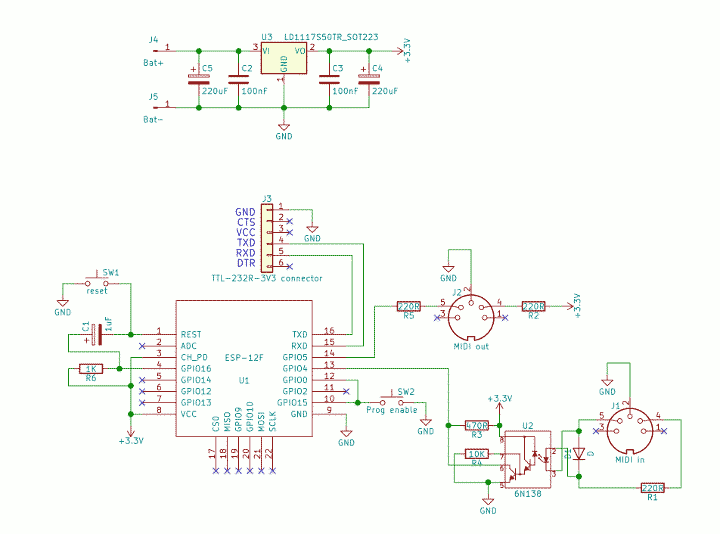
To get an idea of my project’s complexity (or rather lack of it) here’s the schematic:
Footprint assignment is tad painful unless you really know what component packages you will be using. Most of the time I go through various footprints and need to see the preview to understand if it’s what I want. That can be slow - there’s no immediate preview box and clicking icon for preview is not terribly convenient. This is likely thing to change in KiCad v5 which is not too far from first stable release.
Laying out the PCB is fun and trouble free most of the time. The two biggest issues I bumped into were:
- From time to time I manage to move grid reference without even realising it. By accident, and I don’t even understand how.
- This wasn’t an issue in this project but assigning network class (e.g. signal vs power) is quite clumsy. But maybe I’m just missing some workflow trick?
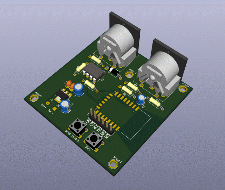
To someone not used to eyeballing CAD drawings (or engineering drawings in general) KiCad’s circuit board 3D preview is indispensable:
Overall I’m really happy with KiCad. With continuous support from CERN and (recently) Digikey KiCad’s future is looks promising.